Catalogue of nanomaterials used in cosmetic products placed on the EU market

The European Commission (EC) has published a catalog of nanomaterials used in cosmetic products on the European Union (EU) market.

On February 5, 2018, the European Union Observatory for Nanomaterials (EUON) published a table linking nanomaterials listed in the catalog to their Registration, Evaluation, Authorization and Restriction of Chemicals (REACH) registration data in the European Chemicals Agency’s (ECHA) database. See https://euon.echa.europa.eu/catalogue-of-cosmetic-ingredients

According to EUON, the linking was done by matching chemical substances in ECHA’s database through their Chemical Abstracts Service (CAS) numbers and/or with the name of the nanomaterial in the catalog. EUON notes that as the registration of nanomaterials under the Cosmetics Regulation and the registration of substances under REACH have different scopes, it is not always possible to have a perfect match. Some catalog entries are more specific in scope than the substances registered under REACH.

EUON cautions that a REACH registration may not specifically cover the nanoforms of the substances used in cosmetics.

http://www.safenano.org/media/127231/nanocatalogue_06_2017_en.pdf

Bolometer Exploits the Thermoelectric Properties of Graphene

The new device, classified as a bolometer, has a fast response time and, unlike most other bolometers, it operates over an extensive range of temperatures. With a relatively low cost and simple design, this device could be scaled up, enabling an extensive range of commercial applications. Researchers have described a graphene-based radiation detector in this week’s edition of Applied Physics Letters, from AIP Publishing.

The discovery of graphene in 2004 was expected to herald a completely new type of technology. “But unfortunately, there are some strong fundamental limitations for this material,” stated Grigory Goblin of Chalmers University of Technology in Sweden. “Nowadays, the real industrial applications of graphene are quite limited.”

Graphene – made up of single sheets of carbon atoms that produce a flat, hexagonal lattice structure – has been employed chiefly for its mechanical properties.

“But our device shows that more fundamental properties can be used in actual applications,” Skoblin said. The new bolometer is based on the thermoelectric properties of graphene. Radiation heats part of the device, prompting electrons to move. The displaced electrons produce an electric field, which develops a voltage difference across the device. An essentially direct measurement of the radiation is thus provided by the change in voltage.

Other devices depend on the generation of electrical current or resistance change brought about by incoming radiation. However, measuring changes in current or resistance need an external power source in order to generate an initial current. According to Skoblin, the mechanism is considered to be much simpler than in other bolometers.

The piece of graphene in the new bolometer is small, hence it is one of the fastest bolometers as it heats up and responds in a rapid manner. Additionally, the device continues to be sensitive to radiation at temperatures up to 200 oC. Standard bolometers usually operate only at cryogenic temperatures.

Other researchers have earlier made graphene bolometers, with improved properties than this new device, however, these models comprise of a double layer of graphene, allowing them to be more difficult to scale, Skoblin said.

Another benefit of the new device is its coating. The researchers earlier developed a method to coat graphene with a dielectric polymer known as Parylene, which offers a good balance of scalability and performance. It is possible to get a better performance by coating with hexagonal boron nitride, Skoblin said, but it is difficult to obtain and the coating techniques are hard to scale up. Other studies indicate that a bolometer with hexagonal boron nitride coating would be less efficient.

The prototype bolometer functions only with microwave radiation at 94 gigahertz, but future designs will indeed widen the frequency range. The researchers next plan to make the device employing chemical vapor deposition to grow bigger pieces of graphene, making way for mass production.

Antifouling Tech Inspired by Carnivorous Plants

A team of chemistry researchers based out of the University of Sydney Nano Institute, led by associate professor Chiara Neto, has devised antifouling surface coatings that do not contain any toxic components, using the surface structure of a carnivorous plant as inspiration.

The need for alternative antifoulants has been on the rise since the ban of tributyltin, a toxic antifouling agent that was commonly used in the past.

Antifouling Agent

The carnivorous Nepenthes pitcher plant, the research team’s inspiration, traps a layer of water on the tiny structures around the rim of its opening, noted The University of Sydney. This creates a slippery layer that causes insects to aquaplane, at which point they slip into the “pitcher” and are digested.

By stopping the initial adhesion of the bacteria, the coating in turn inhibits the formation of a biofilm and the further growth of marine fouling organisms.

Successful Tests

Lab tests demonstrated that these surfaces resisted much of the fouling caused by a common strain of marine bacteria. In comparison, layers of Teflon that went untreated by the coating were completely fouled. To ensure the coating’s ability to hold up under a variety of conditions, the research team also tested the coating in contact with the surface of the ocean.

For this, test surfaces were attached to swimming nets at Watsons Bay baths in Sydney Harbor for seven weeks. Even in this environment, the coating still resisted fouling.

The coatings are also transparent and moldable, which can be useful for underwater cameras and sensors, noted the University of Sydney.

The new coating uses ‘nanowrinkles’ inspired by the carnivorous Nepenthes pitcher plant. The plant traps a layer of water on the tiny structures around the rim of its opening. This creates a slippery layer causing insects to aquaplane on the surface, before they slip into the pitcher where they are digested.

Nanostructures utilise materials engineered at the scale of billionths of a metre — 100,000 times smaller than the width of a human hair. Associate Professor Neto’s group at Sydney Nano is developing nanoscale materials for future development in industry.

Biofouling can occur on any surface that is wet for a long period of time, for example aquaculture nets, marine sensors and cameras, and ship hulls. The slippery surface developed by the Neto group stops the initial adhesion of bacteria, inhibiting the formation of a biofilm from which larger marine fouling organisms can grow.

The interdisciplinary University of Sydney team included biofouling expert Professor Truis Smith-Palmer of St Francis Xavier University in Nova Scotia, Canada, who was on sabbatical visit to the Neto group for a year, partially funded by the Faculty of Science scheme for visiting women.

In the lab, the slippery surfaces resisted almost all fouling from a common species of marine bacteria, while control Teflon samples without the lubricating layer were completely fouled. Not satisfied with testing the surfaces under highly controlled lab conditions with only one type of bacteria the team also tested the surfaces in the ocean, with the help of marine biologist Professor Ross Coleman.

Test surfaces were attached to swimming nets at Watsons Bay baths in Sydney Harbour for a period of seven weeks. In the much harsher marine environment, the slippery surfaces were still very efficient at resisting fouling.

The antifouling coatings are mouldable and transparent, making their application ideal for underwater cameras and sensors.

Story Source:

Materials provided by University of Sydney.


Wirelessly Powering the World Using Triboelectricity

In March 2017, a group of physicists at CNI invented the ultra-simple triboelectric nanogenerator, or U-TENG — a small device made simply of plastic and tape that generates electricity from motion and vibrations. When the two materials are brought together — through clapping your hands or tapping your feet, for example — a voltage is generated that is detected by a wired, external circuit. Electrical energy, by way of the circuit, is then stored in a capacitor or a battery until it’s needed.

Nine months later, in a paper published in the journal Advanced Energy Materials, the researchers have uncovered a wireless version of TENG, called the W-TENG, which greatly expands the applications of the technology.

The W-TENG was engineered under the same premise as the U-TENG, using materials that are so opposite in affinity for electrons that they generate a voltage when brought in contact with each other.

In the W-TENG, plastic was swapped for a multipart fiber made of graphene — a single layer of graphite, or pencil lead — and a biodegradable polymer known as poly-lactic acid (PLA). PLA, on its own, is great for separating positive and negative charges, but not so great at conducting electricity — which is why the researchers paired it with graphene. Kapton tape, the electron-grabbing material of the U-TENG — was replaced with Teflon, a compound known for coating nonstick cooking pans.

“We use Teflon because it has a lot of fluorine groups that are highly electronegative, whereas the graphene-PLA is highly electropositive. That’s a good way to juxtapose and create high voltages,” said Ramakrishna Podila, corresponding author of the study and an assistant professor of physics at Clemson.

To obtain graphene, the researchers exposed its parent compound, graphite, to a high frequency sound wave. The sound wave then act as a sort of knife, slicing the “deck of cards” that is graphite into layer after layer of graphene. This process, called sonication, is how CNI is able to scale up production of graphene to meet the research and development demands of the W-TENG and other nanomaterial inventions in development.

After assembling the graphene-PLA fiber, the researchers exploited additive manufacturing — otherwise known as 3D printing — to pull the fiber into a 3D printer, and the W-TENG was born.

The end result is a device that generates a max voltage of 3000 volts — enough to power 25 standard electrical outlets, or on a grander scale, smart-tinted windows or a liquid crystal display (LCD) monitor. Because the voltage is so high, the W-TENG generates an electric field around itself that can be sensed wirelessly. Its electrical energy, too, can be stored wirelessly in capacitors and batteries.

“It cannot only give you energy, but you can use the electric field also as an actuated remote. For example, you can tap the W-TENG and use its electric field as a ‘button’ to open your garage door, or you could activate a security system — all without a battery, passively and wirelessly,” said Sai Sunil Mallineni, the first author of the study and a Ph.D. student in physics and astronomy.

The wireless applications of the W-TENG are abundant, extending into resource-limited settings, such as in outer space, the middle of the ocean or even the military battlefield. As such, Podila says there is a definite philanthropic use for the team’s invention.

“Several developing countries require a lot of energy, though we may not have access to batteries or power outlets in such settings,” Podila said. “The W-TENG could be one of the cleaner ways of generating energy in these areas.”

The team of researchers, again led by Mallineni, is in the process of patenting the W-TENG through the Clemson University Research Foundation. Professor Apparao Rao, director of the Clemson Nanomaterials Institute, is also in talks with industrial partners to begin integrating the W-TENG into energy applications.

However, before industrial production, Podila says more research is being done to replace Teflon with a more environmentally friendly, electronegative material. A contender for the redesign is MXene, a two-dimensional inorganic compound that has the conductivity of a transition metal and the water-loving nature of alcohols like propanol. Yongchang Dong, another graduate student at CNI, led the work on demonstrating the MXene-TENG, which was published in a Nov. 2017 article in the journal Nano Energy. Herbert Behlow and Sriparna Bhattacharya from CNI also contributed to these studies.

Will the W-TENG make an impact in the realm of alternative, renewable energies? Rao says it will come down to economics,

“We can only take it so far as scientists; the economics need to work out in order for the W-TENG to be successful,” Rao said.

Story Source:

Materials provided by Clemson University.

MXene Nanomaterial Could Enable Efficient Gas Separation for Widespread Use of Hydrogen Fuel

Despite the fact that hydrogen is one of the most highly abundant elements on the planet and an extremely clean source of fuel, its widespread use in the fuel cells of buses, electric cars, and heavy equipment is hindered by the high-cost gas-separation process needed to synthesize pure hydrogen.

However, in the near future, this process might become highly effective and cost-efficient, due to a discovery by an international research team headed by Drexel University, in the United States. The team has unearthed extremely effective gas separation characteristics in a nanomaterial known as MXene that can be combined with the membranes adopted to purify hydrogen.

Although hydrogen exists in a broad range of materials and molecules in nature, the foremost being water (a combination of hydrogen and oxygen), it does not naturally occur on Earth in its pure elemental form. Isolation of hydrogen from the other elements with which it is usually bonded mandates the introduction of an electric current to stimulate and disintegrate the atoms in water molecules or filtering a gaseous mixture including hydrogen, by using a membrane to isolate the hydrogen from hydrocarbons or carbon dioxide.

The procedure of gas separation through membrane is the most efficient and low-cost process. Therefore, in the recent past, scientists have been accelerating their attempts to create membranes with the ability to absolutely and rapidly filter out hydrogen.

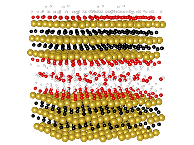
According to a study reported recently in the Nature Communications journal, the use of MXene material in gas-separation membranes can be the most effective method to purify hydrogen gas. The study was headed by Haihui Wang, PhD, a professor from South China University of Technology; and Yury Gogotsi, PhD, a Distinguished University and Bach professor in Drexel’s College of Engineering, in the Department of Materials Science and Engineering. It indicates that the two-dimensional structure of the nanomaterial allows it to selectively filter large gas molecules, while allowing hydrogen to pass through the layers.

In this report we show how exfoliated two-dimensional MXene nanosheets can be used as building blocks to construct laminated membranes for gas separation for the first time. We demonstrated this using model systems of hydrogen and carbon dioxide.

Yury Gogotsi

The Drexel group worked in cooperation with scientists from South China University of Technology, Jilin University (also in China) and Leibniz University of Hannover, in Germany. They described that membranes developed using MXene nanosheets were found to function better than the top-of-the-line membrane materials, with respect to permeability as well as selectivity.

The benefits of MXene over materials that are prevalently used and created for gas separation are that its permeability and also its filtration selectivity are dependent on its chemical composition and structure. Conversely, other membrane materials such as zeolite and graphene perform filtering by means of physically trapping, or filtering, molecules in tiny channels and grids; similar to a net.

The distinctive filtration characteristics of MXene are due to the fact that they are developed through chemical etching of layers from a solid piece of material, known as a MAX phase. This procedure forms a structure that is similar to a sponge, including slit pores of differing sizes. Gogotsi’s Nanomaterials Research Group, which has been collaborating with MXenes from the year 2011, has the potential to predetermine the size of the channels by adopting various kinds of MAX phases and etching them with various chemicals.

The channels can be developed in a manner that renders them chemically active, so that they have the potential to attract, or adsorb, specific molecules when they pass through. Consequently, a MXene membrane acts largely like a magnetic net and can be designed with the ability to trap a broad array of chemicals when they pass through.

This is one of the key advantages of MXenes. We have dozens of MXenes available which can be tuned to provide selectivity to different gasses. We used titanium carbide MXene in this study, but there are at least two dozen other MXenes already available, and more are expected to be studied in the next couple of years – which means it could be developed for a number of different gas separation applications.

Yury Gogotsi

The adaptable two-dimensional material discovered at Drexel in the year 2011 has hitherto exhibited its potential to enhance efficiency of electric storage devices, prevent electromagnetic interference, and also purify water. Gogotsi stated that investigating its gas separation characteristics was the next logical step.

Our work on water filtration, the sieving of ions and molecules, and supercapacitors, which also involves ion sieving, suggested that gas molecules may also be sieved using MXene membranes with atomically thin channels between the MXene sheets. However, we were lacking experience in the gas separation field. This research would not have been possible without our Chinese collaborators, who provided the experience needed to achieve the goal and demonstrated that MXene membranes can efficiently separate gas mixtures.

Yury Gogotsi

For enabling industrial usage of MXene, Gogotsi’s team will further enhance its chemical and temperature stability and durability and reduce its production cost.

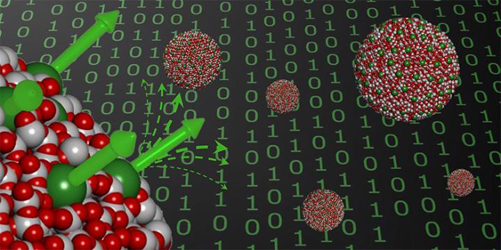
Developing Data Storage Devices with Nanoparticles and Electron Microscopy

Cutting-edge research has shown that iron-platinum nanoparticles – a promising next-generation data storage material – respond to laser pulses by stretching and contracting, according to a new report published in the journal Nature Communications.

Magnetic data storage devices are popular for storing data in almost all aspects of our digital life. While they are likely going to remain vital for the near future, existing technologies are nearing their technical limits. Today’s hard disk drives, for instance, can reach storage densities of many hundred billion bits per square inch and future magnetic devices aren’t projected to exceed much greater than a trillion bits per square inch. New advancements are necessary to take magnetic information storage to the next level. Facing ever-growing demands for data storage, hardware engineers are trying to optimize the density with which these medias can store data.

In the new study, researchers took a major step in the direction of new magnetic storage devices by showing that laser pulses could demagnetize iron-platinum nanoparticles in less than a trillionth of a second, triggering atoms in the material to squeeze together in one direction and stretch apart in a different direction.

The outcome offers the first atomic-level information on the mechanical strain referred to as magnetostriction, which happens when the magnetization is altered in magnetic materials. The phenomenon appears in many ways, including the audible hum of transformers. Prior to the study, the study scientists had thought that these structural shifts occur fairly slowly. However, the new research indicates that ultrafast processes could have major practical implications.

Study author Hermann Dürr, from the Stanford Institute for Materials and Energy Sciences (SIMES), said models of iron-platinum nanoparticle behavior did not predict the fast, fundamental atomic motion seen in the study.

“Although we don’t yet understand the full ramifications of these processes, including them in our calculations could open up new pathways for the development of future data storage technologies.”

Hermann Dürr, Study Author

Co-author Eric Fullerton, director of the Center for Memory and Recording Research at the University of California, said one promising application of the new research involves heat-assisted magnetic recording in hard drives with nanosized grains of materials like iron-platinum.

To reach their conclusion, researchers directed a brief laser pulse onto the nanoparticles, which measured around 50 atoms in diameter. Using femtosecond X-ray flashes, the team was able to see how the laser altered the magnetization of the material, from totally magnetized to mostly demagnetized.

The team repeated the experiment using an ultrafast electron diffraction (UED) instrument, an electron microscopy device that uses a pulsed beam of highly energetic electrons. With this technique, the researchers essentially created a stop-motion movie that revealed how atoms in the nanoparticles reacted to the laser light.

“Only the combination of both methods allowed us to see the full picture of the ultrafast atomic response to laser light,” co-author Alexander Reid, a researcher from SIMES. “The laser pulse alters the magnetization in the material, which, in turn, drives structural changes and causes mechanical strain.”

Xijie Wang, head of a UED initiative at Stanford University’s SLAC National Accelerator Laboratory, where the study was conducted, said the research also showed the power of combining these two analytical methods.

“The high-energy electron beam was absolutely crucial in the determination of the 3-D atomic motions and without X-rays, we wouldn’t have been able to link these motions to the material’s magnetic behavior,” Wang said.